Having a look at the Comparing specs topic, I noticed the Librem 5 has some exposed pads on the back as test points. Does anyone know what can we do with these?
Could the hacker community expand the phones capabilities with mods?
Or can it only be used for flashing/debugging the chips on the L5?
2 Likes
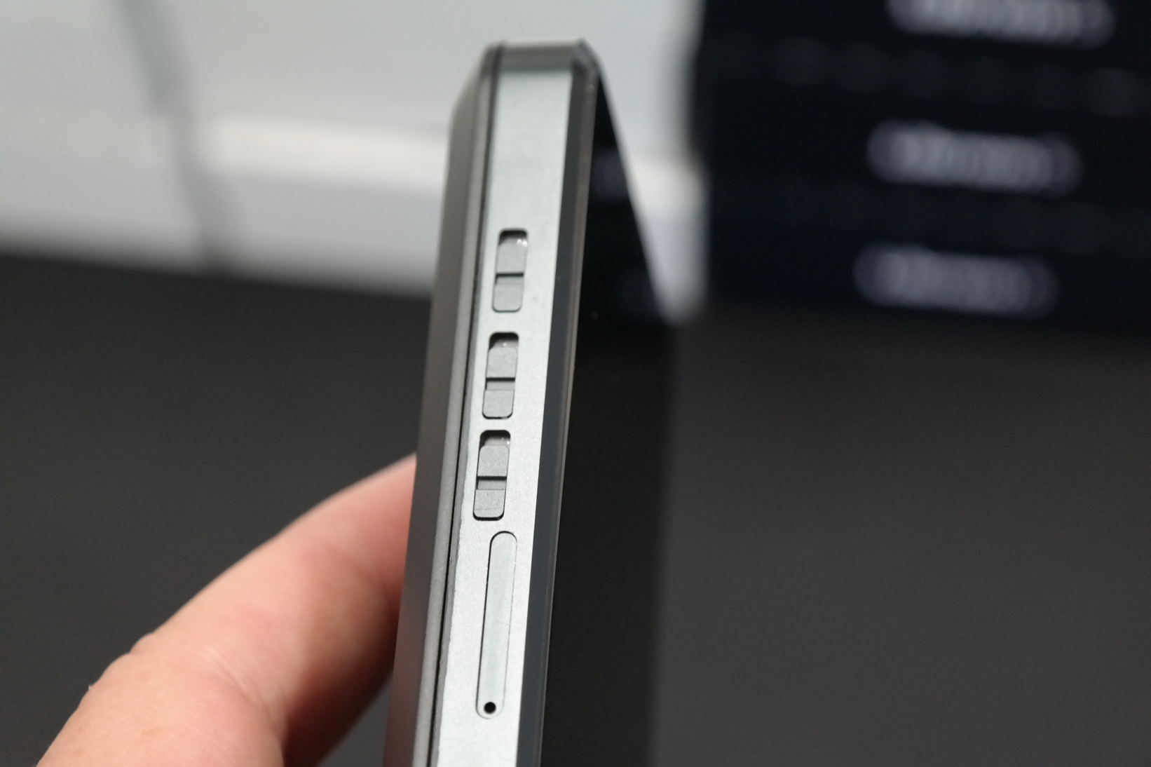
In Dogwood the 20 test points have been consolidated into one group under the WiFi/BT M.2 card, and they are covered with an internal plastic panel, so it looks like you will have cut a hole in that panel to get access.

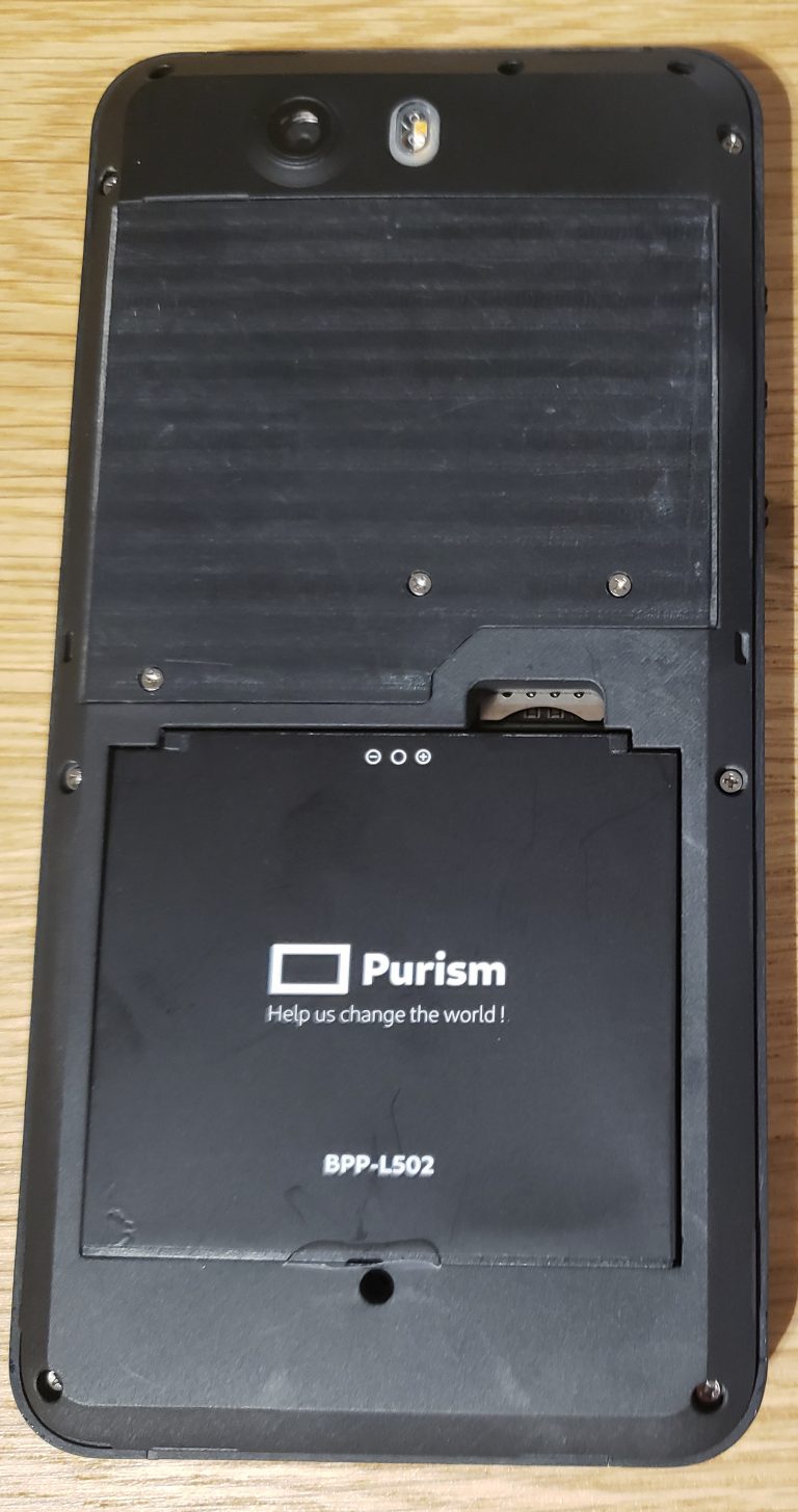
They aren’t pogo pins like in the PinePhone, so you will have to solder wires to them, if you want to use them to add a mod to the Librem 5, but the fact that you have access to USB means that they could be really useful.
I wish that Purism had given us a pogo pin connector to USB for adding mods, but that raises all sorts of security issues. This way, you can paint nail polish with glitter over the screws for that plastic panel covering the PCB and you know that nobody has accessed the phone’s hardware. The other issue is that the Librem 5 at 15.5 mm thick is already too thick to add large mods to the back of the phone, whereas the PinePhone at 9.2 mm thick has more room to add things like a physical keyboard or a 5000 mAh battery to the back.
I’m interested in what are the two boot modes. I assume those boot modes can be used when you have bricked the phone and/or need to flash firmware in the chips.
3 Likes
aww come on @amosbatto
at 15.5 mm thick is already too thick to add large mods to the back of the phone, whereas the PinePhone at 9.2 mm thick has more room to add things
that’s quitter talk ![]() a much more positive way of thinking of it is “a 5mm thick accessory will add only 30% to the thickness, whereas it would cause a 50% increase in thickness on the pinephone”
a much more positive way of thinking of it is “a 5mm thick accessory will add only 30% to the thickness, whereas it would cause a 50% increase in thickness on the pinephone”
From the second link @dean provided it would seem that opening up the area around the hole (that is just ~5mm above the center of the battery recess) would get us the USB connections
A much nicer solution may be if get some people together to place a group order we could get a batch of flex PCB’s (a thin polyamide covered circuit, like the gold coloured one shown in the bottom of the battery cavity) it could pickup the usb pts (by being soldered on), run under that new central plastic piece, connect with the rest of those test points and emerge from the opening between battery cavity and wifi card cavity, then curve up to the back face of the chassis where it would be trapped between the chassis and that final coverplate (which would get some holes drilled in to match the test points or pogo pins on the accessible end of the flex circuit
Edit: Italics
3 Likes
@dean The last two lines of your question are fundamentally linked.
To more directly answer your question, I think its safe to say this phone will will be getting hacked inside out and upside down (not by me, by others faaar more competent) the price point will mean it gets of to a slightly slower start.
Perhaps those that can afford to support this sort of hardware at this price are exactly the group that will make some of the biggest contributions anyway? (not because they are filthy rich, but because its their jam, and they will find a way to afford it)
USB1_DP and USB1_DN are data positive and data negative. USB1_ID could be for host negotiation.
I just checked the schematics and these pads seem to be the same as the ones at the exterior USB-C connector.
The 5 JTAG points are for a system originally used for QA purposes, and early checks during first power-up and basic testing of the components, but as integrated circuit components got more and more powerful it seems they started to incorporate self checking, resetting, calibration, tuning, and firmware flashing.
Its the level you go to when a device like a router is totally and utterly “bricked” because if no hardware damage has been done it can probably be saved (given a heat gun, logic anyliser, reflow oven, and unhealthy amounts of patience) but yea, low level hardware? very interesting for hackers - access to full/official documentation is possibly a difficulty sometimes.
I think POR_B is the reset for the CPU
The 2 UART connections give a serial connection you can watch the debug output of the boot loader and kernel in real time, so if it crashes or hangs, for example before the display drivers are loaded and working, you can work out why. The UART is also used to flash the CPU or component it is attached to.
BOOT_MODE1, BOOT_MODE0 - The state of these pins will be one of the first checks the device does; after verifying the voltage and other essential conditions are ok. Connecting them to GND in different combinations will allow the user to make the device boot into one of four different states. These may be something like Safe mode, Flashing mode, Developer mode, or Self Destruct mode.
The reason this project is so awesome, is the open source bit. Finally we don’t get a multi-national corporation, trying to stop us tweaking, reverse engineering, customizing, or improving the device - which by the way they do because they want their product to have a certain look/sound/feel, so it fits their advertising, so it appeals to the masses, so they sell more stuff.
We get the code, the schematics, and Purism’s blessing to contribute improvements (or make the startup screen display a butt and play fart noises as it boots)
Edit: update about usb connections
3 Likes
Another option would be to add pogo pins to the mod you attach. Assuming that the internal plastic panel does not provide much internal structural stability you would also not need to cut it, only to screw it off.
1 Like
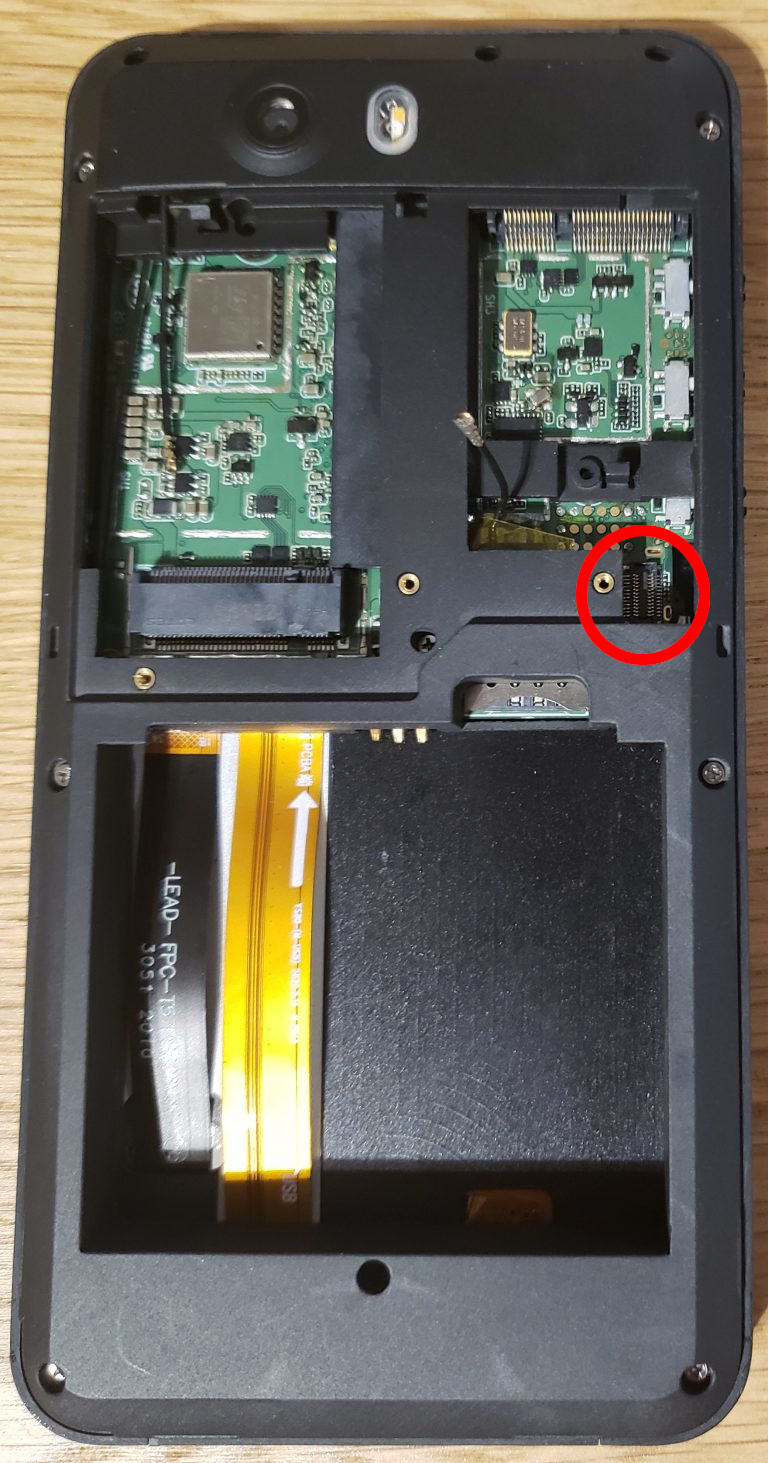
Thanks for the photos @amosbatto. There is a lot of space between the plastic cover and the pads to install spring-loaded connectors and they are easy to get off Digikey.
I don’t know about flexible PCB’s, @mekhos we could just have different PCB’s for B, C, D, and E batches and mount the custom expansion PCB to the plastic cover points.
Direct access to the USB bus is great. @mekhos could we write a ‘driver’ to use the 2 UART like a Raspberry PI, or is it more just for debugging?

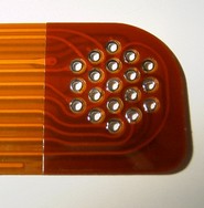
^ this image shows what a flexible printed circuit assembly looks like
^ this image shows the kind of detail was imagining would pick up the contact points of the Librem 5 board.

^ this horrible sketch-over shows the path I was trying to describe, with the green colour meaing below, and magenta meaning above the recently added heat-spreader-chassis-thing
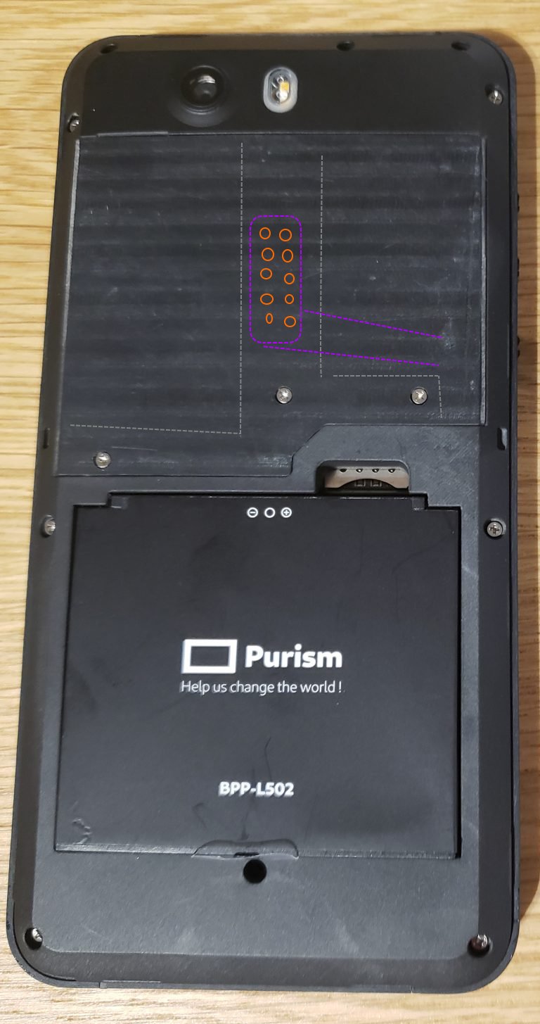
^ this sketch-over shows hidden (dashed) outline of where the final user-accessable contact pads or pogo pins would be, obviously that final coverplate would need clearance hole/holes.
3 Likes
Nice idea with the flexible printed circuit.
You can make it even simpler in Dogwood because all 20 test points are together with 3 rows of 7, 7 and 6 test points:
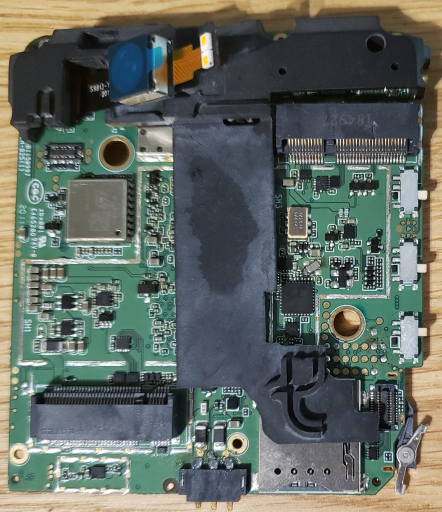
I’m guessing that the black plastic cover over the center of the PCB had a heat spreader under it, but it might just be to stop the user from accidentally touching some chips when changing the M.2 cards. Either way, you can put you flexible printed circuit on top of that.
Yes, I find it a bit mysterious though, because It looks to be plastic…which seams fairly pointless for anything to do with heat except isolating it?
Dang, you see the ring around the hole in the wifi card area? that will be earthed, but look how close some of the test/debug pads get to it! my hands wouldn’t be steady enough to solder that haha.
I also find that attachment at the bottom right corner interesting, I haven’t seen anything like it before, is there a photo of the other side or does anyone know the name?
I thought that metal attachment in the corner was to hook onto something, but it doesn’t look like it does anything in this photo:

I can’t tell why it exists.
 spring or release trigger for the sim car tray? when the tray is inserted that part would rotate about 10degrees CCW, and its lower arm would line up with the hole in photo below.
2 Likes
I do have one suggestion that would make it very easy to use those test points.
Embed pogo pins inside the modem cover.
This would require someone to make a new modem cover with a box reaching down to the PCB, with holes in it for the pins. It would also require the right size and shape of pin. I know you can get pins small enough, but I don’t know about getting them in the ideal shape.
Here’s a sketch.

Obviously, pins in the PCB would be preferable for a lot of reasons. It may be possible to simply solder the pins to the PCB, put the block over them and have it clip to the board then cut a hole in the modem cover, but I wouldn’t have any idea how to surface mount a dozen pogo pins.
5 Likes
It would be nice to see some sort of RAM expansion or eMMC attachment right above the modem/Bluetooth and Wifi card…
Don’t get too focused on the test points, those are useful mostly for debugging - there’s an extension connector under the modem cover which exposes more interesting interfaces, like I2C and NFC.
It’s this one:
I don’t think we have any easy to digest documentation so far, at least you can always find it in the schematic.
3 Likes