New Post: Librem 14 in Pictures

Thanks for the higher resolution photos of the motherboard.

I’m surprised that a double fan was needed, but I’m guessing that 6 CPU cores demands that kind of cooling. From the design, it looks like the heat spreader, heat pipes and two cooling fans are one unit, and the fans can’t be replaced individually. I really hope that Purism sells replacement parts for at least the cooling unit, because I have had two laptops whose fans died in the past, so I know that they can fail.

I would be interested in hearing people’s impressions of the fan noise. Is the fan speed controllable by software?

Can the screen of the L14 be opened 180 degress, so it lies flat on a table?

I’m surprised that stacked RAM slots weren’t used, but I guess that is all part of the effort to make it as thin as possible. I hope that the screws on the bottom have some sort of lock-tight mechanism or are the type that can’t be wholly removed, since that was a problem with the previous design.

I believe it’s controlled by the EC, which means in theory it could be, but Nicole mentions in her Rave post that it’s not implemented yet:

The system fans can not be controlled from user space yet, right now, but they can at least be monitored a bit:

/sys/class/hwmon/hwmon4

We will work further on it.

From the “Librem 14 is Shipping” post:

4 Likes

A connection of solder is just as good as a zero ohm resistor! (And what is the tolerance on that?)

i can see that copper heat pipes are used to transfer the heat from the CPU+iGPU die-combo. i would have liked to see copper fins as well but perhaps at that size it doesn’t matter much.

i hope those lil’ fans have a good few years of life-span in them or at least covered by the 3 year warranty. it just sucks to have an essential hardware component fail just outside of the warranty period. i suggest people grab that 3 year warranty from Purism just for safe measure …

that trackpad/touchpad is huge.

the R-Shift key is so small. does it behave differently out-of-the-box compared to the L-Shift ?

screen looks good. but there is that nasty glare from the ambient … btw how was the ambient lighting condition when these pictures were taken ?

We will know that arrival of the L14 is imminent when the docs show up here

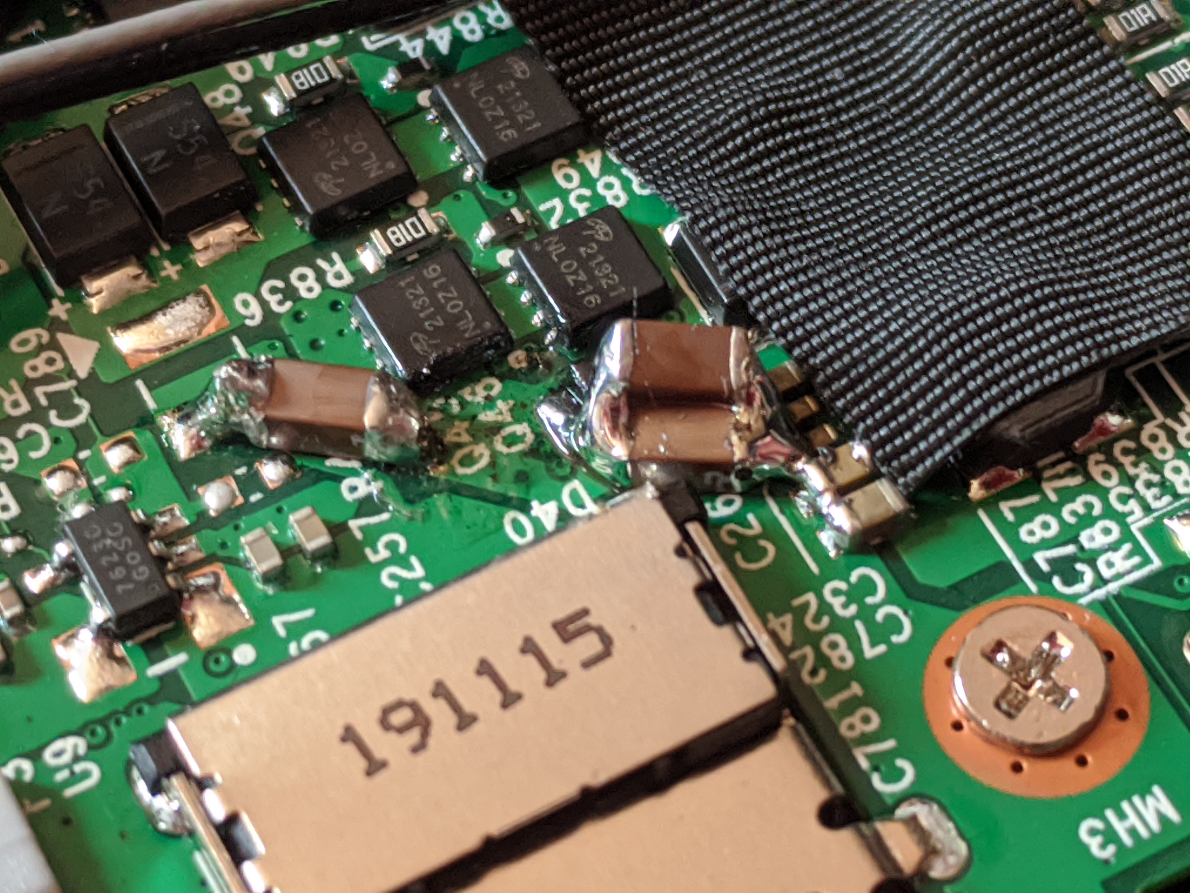
Is my librem 14 famous?

1 Like

It certainly will be if this is the first one in the wild…

2 Likes

That looks really bad.
Now i am considering cancelling my order…
is it 14 you recieved??

@Kyle_Rankin taking apart quality of those solder work, those pictures prove that “final” design of the board is worse than bad…
and actual engineer who did this “patch” really didn’t know what he is doing. such solder is asking for trouble…
such soldering of additional (unplanned) elements , should be done on THT parts instead of SMD, they have small wires that give you option to compose them into electronics in a more aesthetic way, or even misplace them by cable work…

Yep, that is the production model I received from a 100% unaffiliated with purism, plain-old regular order. I absolutely suck at soldering so I can’t pass any judgement on it, but I think the solder on the single capacitor (resistor? idk) has a peak that is less smooth than the blog post so I think this is a separate model than the one originally photographed, making mine not famous :frowning:

What worries me is that all Production will have this flaw.
which makes them very vunreable to damage…

Price of MacBook quality worse than worse china made electronics i saw in my life… :S

That sucks.
I would seriously consider returning the laptop in your position, this is not acceptable for a production board.
I truly hope this is somehow an exception that they had to fix by hand and future production boards will not be this bad.
Either way, what a way to be thanked for an early pre-order

Haha I totally understand your position, but there ain’t no way I’m returning this laptop unless it stops working!

FWIW I think it will be fine in terms of clearance since the solder seems to be shorter than the height of the cards in slots (ram/wifi) but I’m just a programmer, not an electrical engineer, so I don’t know what I’m talking about.

1 Like

@craftkiller any chance we can get a top down picture of the area with a little bit more surrounding area to figure out what they were fixing with those three capacitors?
Would enable me to trace the signals to the connected components and figure out why that hack is or was necessary.

1 Like

Absolutely! I haven’t finished threadlocker bluing my hinge screws yet so its all just sitting open on my desk still. Heres two overhead shots, lmk if you need different/better shots. The black squares are where I blacked out the wifi card’s label.

4 Likes

Forgive my ignorance of laptop mass production, even after being here a few years I’m still learning things. Seeing a hotfix like that not only in the pictures we provided but also this model we sent out, was apparently not expected (which was why it was not originally caught in the first laptops we sent out).

We are looking into this right now to see what’s going on.

11 Likes

Thanks I’ll try to get the parts from the markings on the chips and figure out what is what first, then I’ll try to follow the tracks.
My initial guess would be something with the power management of the USB port, doesn’t seem to be connected to the Ethernet port further down.

What does threadblocker bluing the hinge screws do?


I’ve marked some obvious components in the picture.
It seems like the board got an possible additional USB port available that is not populated, would probably need to be mounted from the other side.
I’d guess the red circle is the SMPS(Switch Mode Power Supply) for the populated USB port with the coil and the two FETs. alternatively the Chip marked IC outside of the red circle could drive that SMPS for the USB port. maybe they just needed those capacitors to keep the SMPS from ringing to much.
If I find those changes on my Laptop as well I’ll try and probe around a bit figuring out what is what.
Initial searches on the net didn’t turn up much useful info about the components.

2 Likes

@Kyle_Rankin to be productive here, and not being accused of being negative:
Fact of fix being put is not a problem. Design flaws happens…

The problem is quality of that fix. this solder in picture is done totally wrong. it’s dangerous to the end user.
We are talking about mobile device, that can be exposed to vibrations, shakes ,etc… that is one factor.
Second factor is image
This is done against any rules of soldering microelectronics.
image
those capacitors should be stacked first, then soldered into one biggest solder point available, then connected with wire into smaller one, both capacitors and wire should be protected with adhesive - there are special UV hardened adhesives for such jobs.
image
same here.
We are not talking about DYI electronic done in basement, we are talking about 1500USD laptop…

That’s the reason of fact that i altered my order resigned from indirection and bought 3 year warranty.
I still believe in Purism, and with Your mission. I hope that till May when my unit will be sent to me your team will learn how to solder stuff :stuck_out_tongue_winking_eye:
Other wise i will sent you a tutorial based on my laptop :stuck_out_tongue_winking_eye:

Enjoy the Beer @Kyle_Rankin :wink:

4 Likes