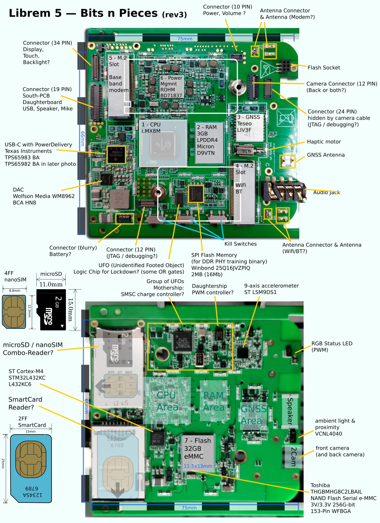
Inspired by an earlier work by @ramnaskohere, with some more details available (e.g. studying all the amazing pictures in the Librem 5 Gallery, using manual OCR), I created this thing here. Click to enlarge.
The SMSC chip is probably for power charging, since SMSC makes those kind of chips. I think that it says “USB” on the second line, so maybe for USB power delivery.
I would assume that the 10 pin connector is for the power, volume up and volume down buttons on the side of the case.
The RGB LED also needs one of the connectors. I would assume that the RGB LED will be at the top, so maybe it uses the 12 pin connector at the top, but that seems like a lot of pins just for a LED.
For ignoramuses such as myself, info about the placement and orientation of those two pictures relative to the rest of the phone would be helpful. Like, what is up/down, right/left, front/back of the phone in relation to each of the two pictures?
Are the two pictures showing two sides of the same green thingy inside the phone?
Yes, two sides of one coin… err… PCB.
To see how it’s oriented in the phone, look at the linked gallery. The CPU und Flash face backwards. The jack faces upwards.
Indeed, using some imagination, one can find the L432KC6 identifier and ST logo.
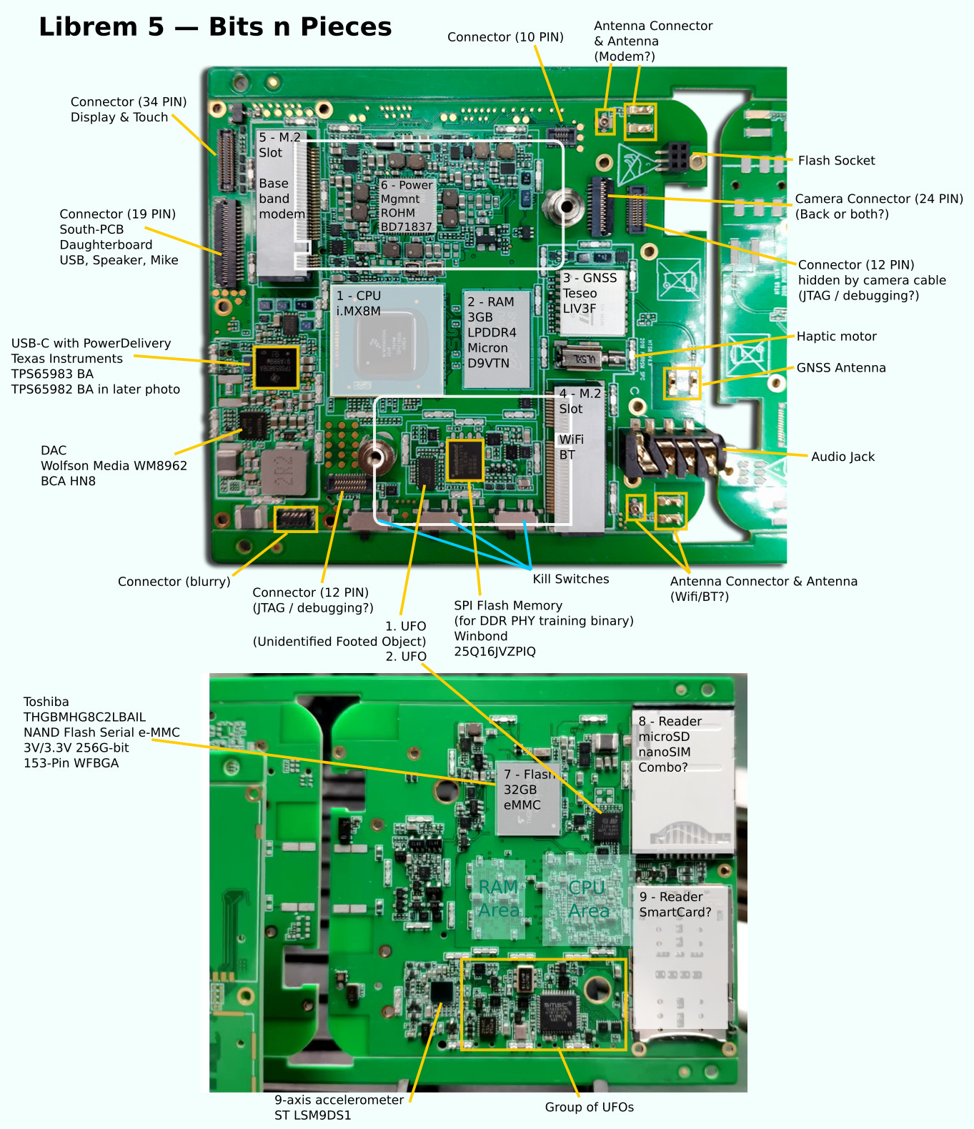
Thus, the 2. UFO is indeed the Cortex-M4 STM32L432KC, as you first noted here.
My reasoning for the readers was: Have a concave top to allow pulling one card. Have a push/eject mechanism for two cards. I admit this could be totally wrong
Placement of the M4 chip hints you are right.
What baffles me is that we have
M4 core inside the CPU + extra Flash chip (winbond) for the PHY training
M4 core including Flash memory as extra chip to control the smartcard reader
On the SMSC chip: Note that I identified the USB+PD chip and the ROHM Power Management chip (surrounded by lots of capacitors?) you also found before.
You’re likely correct, I’m just surprised that charge control would not be a part of the Power Management chip.
On the connectors:
The front camera (hole) is on the top right.
I’m pretty certain the ambient/proximity sensor sits right next to it.
Then, there are four pads for the speaker in the middle.
On the left, there should be the RGB LED.
Amusingly, this is basically the the layout my current S3 has, which I had as an example when requesting a status LED two years ago…
On the matter of led and speaker for the front: I still don’t get the four big silber contacts in the middle. I find in kind of unusual but they would be enough to be contact pads for led and speaker. ground, power, speaker signal and led data. this would imply a multi clour led with IC as thes only need one data line instead of one power line per colure. If the small black parts are light and distance sensors all the front part would be covered without using a connector.
And most displays i have seen have separate connectors for lcd and touchscreen. Thought i have mostly repaired iphones but also some android devices. And as far as i know the devkit also has sperate connectors
So i’m still think one of the connectors is need for that. The one on the top by the camera could be used. the flex cable could be folded around the pcb edge on the camera cut out and the camera an cable could be placed ontop.
AFAIK, sometimes not all pads are used for electric reasons.
I assume two of the pads just hold the speaker.
I think the same is true for the haptic motor.
Hmm yeah i forgot about the solder pads to hold big components in place. And i assumed that als fixed components are on the pic.
So i‘m with you. Speaker contacts plus fixation solder pads are a likely option.
But i hope for an non solder speaker as it is as part which likely needs replacement after some years of use.
Debugport:
I think the 6 pins are enough for debug flash etc and it is the only reasonable connector for this. I don’t think any other connector is meant for such use.
The group of ufos is next to the hardware killswitches.
also as on the left of the front side of the group of ufos is the accelorator, so I guess the left of the group of ufos is for the lockdown mode while on the right the group of ufos might kill the wifi / bt hw based?
I think there are dual (sim and sd crad) slots which have both cards on one tray which slides in from the out side. So i guess every thing will be accessible from the outside.
You know what? 10 pins for power and volume is also plenty.
People say the buttons look translucent
Wouldn’t it be awesome to have some back-lit buttons, showing the kill swich state or indicating that the battery needs charging (power button)?
Only lighting up for a few seconds when activating the device.
Power and volume buttons do a fancy animation while charging … would be fun